
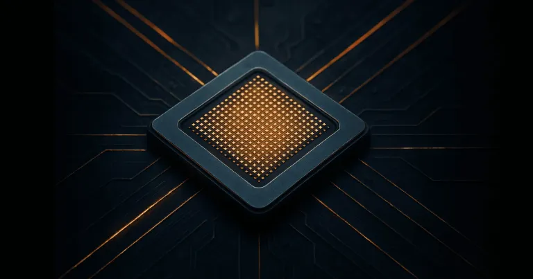
 Technology peripheralsIt Industry144-core, 3D-stacked SRAM: Fujitsu details next-generation data center processor MONAKA
144-core, 3D-stacked SRAM: Fujitsu details next-generation data center processor MONAKA

This website reported on July 28 that according to foreign media TechRader, Fujitsu introduced in detail the FUJITSU-MONAKA (hereinafter referred to as MONAKA) processor planned to be shipped in 2027. MONAKA CPU is based on the "cloud native 3D many-core" architecture and adopts the Arm instruction set. It is oriented to the data center, edge and telecommunications fields. It is suitable for AI computing and can implement mainframe-level RAS1.

- Thanks to technologies such as ultra-low voltage (ULV) process, the CPU can achieve 2 times the energy efficiency of competing products in 2027, and cooling does not require water cooling ;
- In addition, the application performance of this processor can also reach 2 times that of its opponents.
In terms of instructions, the vector instruction set equipped with MONAKA has been upgraded to SVE2, which can better meet the needs of the AI and HPC fields; in addition, the CPU also adds support for confidential secure computing.
MONAKA supports dual-socket, each CPU contains 144 Armv9 architecture cores.
Each CPU includes a central IO Die and four 3D vertically stacked complexes. The bottom is a silicon interposer (Si Interposer) and packaging layer that connects various parts;
Each complex is processed by The processor core Core Die is combined with the LLC last-level cache SRAM Die. The Core Die is located above the SRAM Die.

Fujitsu said that the 2nm part of its processor only accounts for 30% of the overall die area, helping to achieve better cost-effectiveness.
Since the on-chip 3D stacked SRAM cache can already provide excellent bandwidth, the MONAKA processor abandoned the HBM memory used by the previous generation product - the A64FX used in the "Fuyue" supercomputer - for off-chip storage, and adopted More traditional 12-channel DDR5 memory .
The processor also provides PCIe 6.0 lanes and supports CXL 3.0 interconnect.

The above is the detailed content of 144-core, 3D-stacked SRAM: Fujitsu details next-generation data center processor MONAKA. For more information, please follow other related articles on the PHP Chinese website!

 Top 21 Developer Newsletters to Subscribe To in 2025Apr 24, 2025 am 08:28 AM
Stay informed about the latest tech trends with these top developer newsletters! This curated list offers something for everyone, from AI enthusiasts to seasoned backend and frontend developers. Choose your favorites and save time searching for rel
 Serverless Image Processing Pipeline with AWS ECS and LambdaApr 18, 2025 am 08:28 AM
This tutorial guides you through building a serverless image processing pipeline using AWS services. We'll create a Next.js frontend deployed on an ECS Fargate cluster, interacting with an API Gateway, Lambda functions, S3 buckets, and DynamoDB. Th
 CNCF Arm64 Pilot: Impact and InsightsApr 15, 2025 am 08:27 AM
This pilot program, a collaboration between the CNCF (Cloud Native Computing Foundation), Ampere Computing, Equinix Metal, and Actuated, streamlines arm64 CI/CD for CNCF GitHub projects. The initiative addresses security concerns and performance lim
 Building a Network Vulnerability Scanner with GoApr 01, 2025 am 08:27 AM
This Go-based network vulnerability scanner efficiently identifies potential security weaknesses. It leverages Go's concurrency features for speed and includes service detection and vulnerability matching. Let's explore its capabilities and ethical


Hot AI Tools

Undresser.AI Undress
AI-powered app for creating realistic nude photos

AI Clothes Remover
Online AI tool for removing clothes from photos.

Undress AI Tool
Undress images for free

Clothoff.io
AI clothes remover

Video Face Swap
Swap faces in any video effortlessly with our completely free AI face swap tool!

Hot Article
Hot Tools

PhpStorm Mac version
The latest (2018.2.1) professional PHP integrated development tool

Atom editor mac version download
The most popular open source editor

WebStorm Mac version
Useful JavaScript development tools

SecLists
SecLists is the ultimate security tester's companion. It is a collection of various types of lists that are frequently used during security assessments, all in one place. SecLists helps make security testing more efficient and productive by conveniently providing all the lists a security tester might need. List types include usernames, passwords, URLs, fuzzing payloads, sensitive data patterns, web shells, and more. The tester can simply pull this repository onto a new test machine and he will have access to every type of list he needs.

EditPlus Chinese cracked version
Small size, syntax highlighting, does not support code prompt function

