 Technology peripherals
 AI
AI Here comes the transistor lifeline: 3D stacked CMOS, will Moore's Law continue for another 10 years?
Here comes the transistor lifeline: 3D stacked CMOS, will Moore's Law continue for another 10 years?
The transistor is known as "the greatest invention of the 20th century."
# Its emergence laid the foundation for the production of integrated circuits, microprocessors and computer memory.
#In 1965, the proposal of "Moore's Law" became the golden rule of the semiconductor industry for decades.
It shows that every 18 to 24 months, the number of transistors packaged on a microchip will double, and the performance of the chip will also follow double.

However, with the continuous introduction of new process nodes, the number of atoms in the transistor has become less and less, and various Physical extreme limits restrict the further development of Moore's Law.
# Some people even think that Moore’s Law is over.
Therefore, in order to "save" Moore's Law, engineers have to change the transistor structure, continue to reduce area and power consumption, and improve its performance.
In the second half of the 20th century, planar transistor design (Planar Transistor) was mainly popular. Entering the 2010s, 3D fin-shaped devices gradually replaced flat designs.
#Now, a completely new transistor design structure, the gate-all-around transistor (GAA), is the successor to FinFET and is about to enter production.

But, we must look further. Because even with this new transistor architecture RibbonFET proposed by Intel, our ability to reduce size has limitations.
Believe that 3D stacked complementary metal oxide semiconductor (CMOS) or CFET (complementary field effect transistor) will be the extension of Moore’s Law to the next ten years. The key to the year.
The evolution of the transistor
Every metal oxide semiconductor field effect transistor (MOSFET) has the same set of basic components:
Gate stack, channel region, source, drain
The source and drain are chemically doped so that they are either rich in mobile electrons (n-type) or lacking in them (p-type). The channel region has the opposite doping to the source and drain.
In the planar version of the transistor in advanced microprocessors before 2011, the gate stack of the MOSFET was just above the channel area. Project the electric field into the channel region.
Applying a large enough voltage to the gate (relative to the source) will form a layer of mobile charge carriers in the channel area, so that Let current flow between source and drain.

In order to reduce the size of planar transistor designs, a "short channel effect" has become the focus of physicists.
#Because as process technology continues to improve, the width of the gate electrode in the transistor is squeezed smaller and smaller. You know, when the gate is lower than 20nm, the current will be out of control, and the source current will penetrate the gate and directly reach the drain.
#At this time, "leakage" will occur, which will cause the chip's energy consumption to rise sharply.

In order to solve this problem, a new FinFET transistor technology has been proposed. It wraps the gate around a channel on three sides to provide better static control.
FinFET reduces power consumption by approximately 50% at the same performance level as previous generation planar architectures. FinFETs also switch faster, delivering a 37% performance improvement.
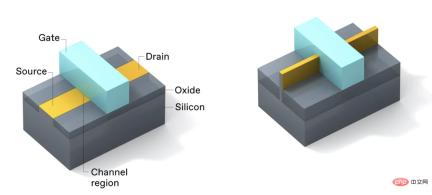
In 2011, Intel introduced FinFET on its 22nm node and used it in the third The production of generation Core processors.
#Since then, FinFET has become the workhorse of Moore’s Law.
#However, we also lost something when we moved to FinFET.
#In planar devices, the width of the transistor is defined by photolithography, so it is a highly flexible parameter.
#But in FinFET, transistor width comes in discrete increments, one fin at a time. This property is often called fin quantization.
#Despite the flexibility of FinFETs, fin quantization remains an important design constraint. The design rules surrounding it, and the desire to add more fins to improve performance, increase the overall area of a logic cell and complicate the interconnect stack that turns a single transistor into a complete logic circuit.
# It also increases the capacitance of the transistor, thereby reducing its switching speed. So while FinFET has served us well as an industry workhorse, a new, more refined approach is needed.
# It’s this approach that led physicists to the invention of the upcoming 3D transistor, the RibbonFET.

In a RibbonFET, the gate surrounds the transistor channel area to enhance control of charge carriers. The new structure also enables better performance and more refined optimization.
Specifically, the gate completely surrounds the channel, providing tighter control over the charge carriers within the channel, which are now made of nanoscale Silicon ribbons form.
Using these nanoribbons (nanosheets), it is again possible to use photolithography to change the width of the transistor as needed.

Once the quantization constraints are removed, it is possible to generate an appropriately sized width for the application. This allows us to balance power, performance and cost.
#More importantly, by stacking and operating in parallel, devices can drive more current, improving performance without increasing area.
# Therefore, Intel believes that RibbonFET is the best choice to achieve higher performance at reasonable power.
They will introduce the RibbonFET structure on the Intel 20A process in 2024.

3D stacked CMOS
One thing that planar, FinFET and RibbonFET transistors have in common is that they all Using CMOS technology, as mentioned earlier, CMOS consists of n-type and p-type transistors. This technology became mainstream in the 1980s because it draws much less current than other alternatives. Less current means higher operating frequencies and higher transistor density.
To date, all CMOS technologies have placed standard pairs of NMOS and PMOS transistors side by side. However, in the keynote speech of the 2019 IEEE International Electronic Components Conference (IEDM), a concept of "3D stacked" transistors was proposed, placing NMOS transistors on top of PMOS transistors.
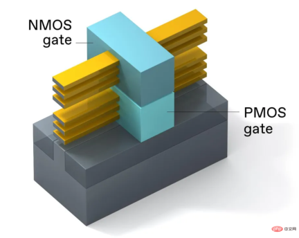
At IEDM 2020, the first inverter designed using this 3D technology for logic circuits was presented device. 3D stacked CMOS effectively reduces the inverter footprint by half, doubling the transistor area density and further pushing the limits of Moore's Law.
3D stacked CMOS structure, placing the PMOS device on top of the NMOS device, with a total area the same as that of a RibbonFET. NMOS and PMOS gates use different metal materials
To utilize 3D stacked CMOS, there are many process integration challenges to be solved, some of which involve CMOS processing and manufacturing. limit.
How to achieve it? The fabrication of self-aligned 3D CMOS begins with silicon wafers. On the wafer, we deposit layer after layer of silicon and silicon germanium, a structure called a "superlattice." Photolithographic patterns are then used to cut away part of the superlattice, leaving a fin-like structure. Superlattice crystals provide a strong support structure for subsequent development processes.
Next, a "fake" polysilicon is placed on the superlattice to protect the former from the next operation. This step, known as a vertically stacked dual source/drain process, grows phosphorus-doped silicon on both ends of the top nanoribbon (future NMOS site) while selectively growing doped silicon on the bottom nanoribbon (future PMOS site). Boron silicon germanium. Afterwards, a dielectric is placed around the power sources to isolate them from each other through electrical discharge.
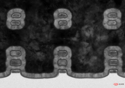
3D stacking effectively doubles the density of CMOS transistors per square millimeter, with actual density depending on the logic cells involved complexity.
#Finally comes the construction of the door. First remove the previously installed false door to expose the silicon nanoribbons. Next, only the silicon germanium is etched away, releasing a pile of parallel silicon nanoribbons, which is the channel region of the transistor.
Then a very thin insulating layer is coated on all four sides of the nanoribbon. This insulating layer has a very high dielectric constant. Nanoribbon channels are so small that they cannot be chemically coated as efficiently as planar transistors.
Surround the bottom nanoribbon with a metal to form a p-doped channel, and the top nanoribbon forms an n-doped channel with another nanoribbon. In this way, the gate stack is constructed and the two transistors are installed.
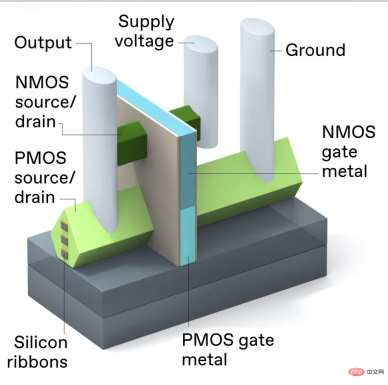
This process may look complicated, but it is better than another technique (sequential 3D stacking). If the latter is used, the NMOS device and the PMOS device are mounted on separate wafers, and then the two are brought together and the PMOS layer is transferred to the NMOS wafer. The self-aligned 3D stacking method has fewer processing steps and can more strictly control manufacturing costs.
#And more importantly, this self-alignment method also avoids alignment errors that may occur when connecting two wafers. Making all the required connections to 3D stacked CMOS is very challenging. Power connections will be required from the device stack below. By design, the NMOS device [top] and the PMOS device [bottom] have separate source/drain contacts, but both devices share a common gate.
It is worth noting that the vertical spacing between NMOS and PMOS needs to be optimized: if it is too short, it will increase the parasitic capacitance, if it is too long, it will Increase the resistance of the interconnect between two devices. Either extreme situation will cause the circuit to slow down and consume more power.
Many design studies, such as the one presented by the American TEL Research Center at the IEDM 2021 conference, propose to provide all necessary interconnects within the limited space of 3D CMOS, and doing so will not significantly Increase the area of the logic cells they form. The research shows that there are many opportunities for innovation in finding the best interconnect options.
The future of Moore’s Law
With strip field effect transistors and 3D CMOS, we have a clear path to continue the life of Moore’s Law The route can be extended at least until 2024 and beyond.
#In a 2005 interview, Gordon Moore, the creator of Moore's Law, admitted that "I am surprised from time to time by the progress that has been made."
#########################He said, “There were times along the way that I thought we had reached the end, but our creative engineers came up with ways to overcome the difficulties. Method." ################## As the transistor manufacturing process passes through FinFET, and with continuous optimization, it comes to the RibbonFET era, and finally moves towards the 3D stacked CMOS process, we It is expected that Mr. Gordon Moore will be surprised soon. #########
The above is the detailed content of Here comes the transistor lifeline: 3D stacked CMOS, will Moore's Law continue for another 10 years?. For more information, please follow other related articles on the PHP Chinese website!
 Convert Text Documents to a TF-IDF Matrix with tfidfvectorizerApr 18, 2025 am 10:26 AM
This article explains the Term Frequency-Inverse Document Frequency (TF-IDF) technique, a crucial tool in Natural Language Processing (NLP) for analyzing textual data. TF-IDF surpasses the limitations of basic bag-of-words approaches by weighting te
 Building Smart AI Agents with LangChain: A Practical GuideApr 18, 2025 am 10:18 AM
Unleash the Power of AI Agents with LangChain: A Beginner's Guide Imagine showing your grandmother the wonders of artificial intelligence by letting her chat with ChatGPT – the excitement on her face as the AI effortlessly engages in conversation! Th
 Mistral Large 2: Powerful Enough to Challenge Llama 3.1 405B?Apr 18, 2025 am 10:16 AM
Mistral Large 2: A Deep Dive into Mistral AI's Powerful Open-Source LLM Meta AI's recent release of the Llama 3.1 family of models was quickly followed by Mistral AI's unveiling of its largest model to date: Mistral Large 2. This 123-billion paramet
 What is Noise Schedules in Stable Diffusion? - Analytics VidhyaApr 18, 2025 am 10:15 AM
Understanding Noise Schedules in Diffusion Models: A Comprehensive Guide Have you ever been captivated by the stunning visuals of digital art generated by AI and wondered about the underlying mechanics? A key element is the "noise schedule,&quo
 How to Build a Conversational Chatbot with GPT-4o? - Analytics VidhyaApr 18, 2025 am 10:06 AM
Building a Contextual Chatbot with GPT-4o: A Comprehensive Guide In the rapidly evolving landscape of AI and NLP, chatbots have become indispensable tools for developers and organizations. A key aspect of creating truly engaging and intelligent chat
 Top 7 Frameworks for Building AI Agents in 2025Apr 18, 2025 am 10:00 AM
This article explores seven leading frameworks for building AI agents – autonomous software entities that perceive, decide, and act to achieve goals. These agents, surpassing traditional reinforcement learning, leverage advanced planning and reasoni
 What's the Difference Between Type I and Type II Errors ? - Analytics VidhyaApr 18, 2025 am 09:48 AM
Understanding Type I and Type II Errors in Statistical Hypothesis Testing Imagine a clinical trial testing a new blood pressure medication. The trial concludes the drug significantly lowers blood pressure, but in reality, it doesn't. This is a Type
 Automated Text Summarization with Sumy LibraryApr 18, 2025 am 09:37 AM
Sumy: Your AI-Powered Summarization Assistant Tired of sifting through endless documents? Sumy, a powerful Python library, offers a streamlined solution for automatic text summarization. This article explores Sumy's capabilities, guiding you throug


Hot AI Tools

Undresser.AI Undress
AI-powered app for creating realistic nude photos

AI Clothes Remover
Online AI tool for removing clothes from photos.

Undress AI Tool
Undress images for free

Clothoff.io
AI clothes remover

AI Hentai Generator
Generate AI Hentai for free.

Hot Article

Hot Tools

MinGW - Minimalist GNU for Windows
This project is in the process of being migrated to osdn.net/projects/mingw, you can continue to follow us there. MinGW: A native Windows port of the GNU Compiler Collection (GCC), freely distributable import libraries and header files for building native Windows applications; includes extensions to the MSVC runtime to support C99 functionality. All MinGW software can run on 64-bit Windows platforms.

SublimeText3 English version
Recommended: Win version, supports code prompts!

SublimeText3 Chinese version
Chinese version, very easy to use

SAP NetWeaver Server Adapter for Eclipse
Integrate Eclipse with SAP NetWeaver application server.

PhpStorm Mac version
The latest (2018.2.1) professional PHP integrated development tool


