 Technology peripherals
 It Industry
 Sources say Intel is considering introducing DSA technology to assist High NA EUV lithography to improve pattern quality
Sources say Intel is considering introducing DSA technology to assist High NA EUV lithography to improve pattern quality
According to news from this site on April 19, foreign media SemiAnalysis and The Elec reported that Intel is considering introducing directional self-assembly DSA technology to assist in future High NA EUV lithography nodes.
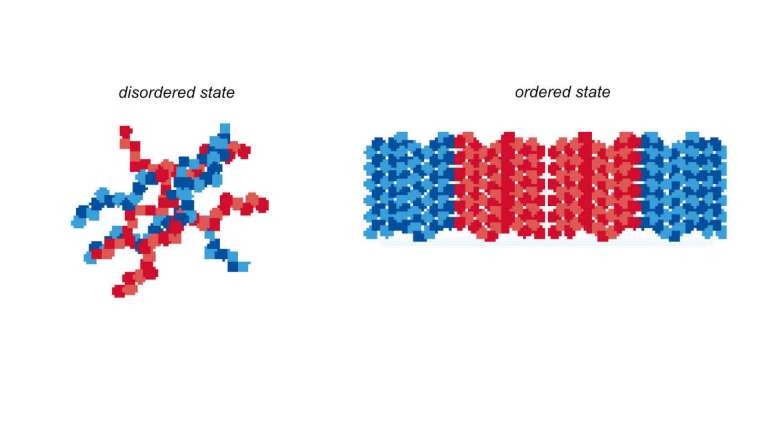
DSA is one of the new patterning technologies that is considered to be able to partially replace traditional photolithography (note on this site: the other is nanoimprinting NIL), which utilizes the molecular properties of chimeric copolymers to achieve Patterning. It is generally considered to be suitable for assisting traditional photolithography rather than being used independently.

SemiAnalysis believes that a big problem facing High NA EUV lithography is the consistency of critical dimensions (CD, a key indicator for measuring the sophistication of semiconductor processes). The contradiction between the timing irradiation dose and the wafer throughput of the photolithography machine leads to the variation of CD. In order to solve this problem, a series of measures need to be taken to improve the stability of the lithography machine and the uniformity of the lithography dose.
If the wafer fab needs to have a good patterning effect while ensuring critical dimensions, then the irradiation dose must be increased. This will slow down the lithography process, reduce the wafer throughput of the lithography machine, and increase the cost burden of the wafer fab.
If the fab runs the lithography machine at a higher throughput, it means that the quality of the lithography pattern decreases as the irradiation dose decreases. At this point, DSA directional self-assembly technology can come into play to repair feature errors on the photolithography pattern.
The introduction ofDSA directional self-assembly can improve the quality of photolithography patterns while reducing the irradiation dose and improving the wafer throughput of the photolithography machine, making High NA EUV lithography more cost-effective sex.
In addition to DSA, Intel is also considering introducing pattern shaping technology into High NA EUV lithography.
Applied Materials released the Centura Sculpta pattern shaping system early last year. This system can precisely modify the characteristic patterns on the wafer in a direction and reduce the number of photolithography times for key layers. It also has the effect of improving the quality of photolithography patterns.
Samsung Electronics also has the intention to introduce the Centura Sculpta system.
Intel researcher Mark Phillip emphasized: "In order to improve the efficiency of the lithography process, it is necessary to introduce equipment other than the lithography machine to supplement it."
The above is the detailed content of Sources say Intel is considering introducing DSA technology to assist High NA EUV lithography to improve pattern quality. For more information, please follow other related articles on the PHP Chinese website!
 Top 21 Developer Newsletters to Subscribe To in 2025Apr 24, 2025 am 08:28 AM
Stay informed about the latest tech trends with these top developer newsletters! This curated list offers something for everyone, from AI enthusiasts to seasoned backend and frontend developers. Choose your favorites and save time searching for rel
 Serverless Image Processing Pipeline with AWS ECS and LambdaApr 18, 2025 am 08:28 AM
This tutorial guides you through building a serverless image processing pipeline using AWS services. We'll create a Next.js frontend deployed on an ECS Fargate cluster, interacting with an API Gateway, Lambda functions, S3 buckets, and DynamoDB. Th
 CNCF Arm64 Pilot: Impact and InsightsApr 15, 2025 am 08:27 AM
This pilot program, a collaboration between the CNCF (Cloud Native Computing Foundation), Ampere Computing, Equinix Metal, and Actuated, streamlines arm64 CI/CD for CNCF GitHub projects. The initiative addresses security concerns and performance lim


Hot AI Tools

Undresser.AI Undress
AI-powered app for creating realistic nude photos

AI Clothes Remover
Online AI tool for removing clothes from photos.

Undress AI Tool
Undress images for free

Clothoff.io
AI clothes remover

Video Face Swap
Swap faces in any video effortlessly with our completely free AI face swap tool!

Hot Article

Hot Tools

Safe Exam Browser
Safe Exam Browser is a secure browser environment for taking online exams securely. This software turns any computer into a secure workstation. It controls access to any utility and prevents students from using unauthorized resources.

SublimeText3 Mac version
God-level code editing software (SublimeText3)

mPDF
mPDF is a PHP library that can generate PDF files from UTF-8 encoded HTML. The original author, Ian Back, wrote mPDF to output PDF files "on the fly" from his website and handle different languages. It is slower than original scripts like HTML2FPDF and produces larger files when using Unicode fonts, but supports CSS styles etc. and has a lot of enhancements. Supports almost all languages, including RTL (Arabic and Hebrew) and CJK (Chinese, Japanese and Korean). Supports nested block-level elements (such as P, DIV),

Notepad++7.3.1
Easy-to-use and free code editor

WebStorm Mac version
Useful JavaScript development tools


