 Technology peripherals
 AI
AI An overview of the three mainstream chip architectures for autonomous driving in one article
An overview of the three mainstream chip architectures for autonomous driving in one article

The current mainstream AI chips are mainly divided into three categories: GPU, FPGA, and ASIC. Both GPU and FPGA are relatively mature chip architectures in the early stage and are general-purpose chips. ASIC is a chip customized for specific AI scenarios. The industry has confirmed that CPUs are not suitable for AI computing, but they are also essential in AI applications.

GPU solution
Architecture comparison between GPU and CPU
CPU follows the von Neumann architecture, the core of which is the storage of programs/data and serial sequential execution. Therefore, the CPU architecture requires a large amount of space to place the storage unit (Cache) and the control unit (Control). In contrast, the computing unit (ALU) only occupies a small part, so the CPU is limited in large-scale parallel computing. Limitations are relatively better at handling logical controls.
GPU (GraphicsProcessing Unit), i.e. graphics processor, is a large-scale parallel computing architecture composed of a large number of computing units. It was originally separated from the CPU specifically to process image parallelism. Compute data, designed to handle multiple parallel computing tasks simultaneously. The GPU also contains basic computing units, control units and storage units, but the architecture of the GPU is very different from that of the CPU. Its architecture diagram is shown below.
Compared with the CPU, less than 20% of the CPU chip space is ALU, while more than 80% of the GPU chip space is ALU. That is, the GPU has more ALUs for data parallel processing.
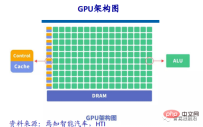
The difference between GPU and CPU
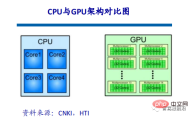
CPU Consisting of a few cores optimized for sequential serial processing, the GPU has a massively parallel computing architecture composed of thousands of smaller, more efficient cores designed for simultaneous processing Designed for multi-tasking.
The reason why CPU and GPU are very different is due to their different design goals. They respectively target two different application scenarios. The CPU needs strong versatility to handle various data types. At the same time, it requires logical judgment and introduces a large number of branch jumps and interrupt processing. All of these make the internal structure of the CPU extremely complex. The GPU faces large-scale data with highly unified types and no dependencies on each other and a pure computing environment that does not need to be interrupted.
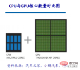
A brief description of GPU acceleration technology
For deep learning, current hardware acceleration mainly relies on the use of graphics processing units. Compared with traditional CPUs, GPUs have several orders of magnitude more core computing power and are easier to perform parallel calculations.
The many-core architecture of the GPU contains thousands of stream processors, which can perform operations in parallel and greatly shorten the calculation time of the model. As companies such as NVIDIA and AMD continue to promote large-scale parallel architecture support for their GPUs, GPUs for general computing have become an important means of accelerating parallel applications.
Currently GPU has developed to a relatively mature stage. Using GPU to train deep neural networks can give full play to its efficient parallel computing capabilities of thousands of computing cores. In scenarios where massive training data is used, the time spent is greatly shortened and fewer servers are occupied. If properly optimized for a proper deep neural network, a GPU card can be equivalent to the computing power of dozens or even hundreds of CPU servers. Therefore, GPU has become the industry's preferred solution for deep learning model training.
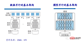
When the scale of the trained model is relatively large, the training of the model can be accelerated through data parallelism. Data parallelism can segment the training data and use multiple model instances to process multiple chunks of data. Train at the same time. In the implementation of data parallelism, since the same model and different data are used for training, the bottleneck affecting model performance lies in parameter exchange between multiple CPUs or multiple GPUs. According to the parameter update formula, the gradients calculated by all models need to be submitted to the parameter server and updated to the corresponding parameters. Therefore, the division of data slices and the bandwidth of the parameter server may become bottlenecks that limit the efficiency of data parallelism.
In addition to data parallelism, model parallelism can also be used to accelerate model training. Model parallelism refers to splitting a large model into several shards, which are held by several training units respectively. Each training unit cooperates with each other to complete the training of the large model.
GPU accelerated computing
GPU accelerated calculation Computing is the use of both graphics processing units (GPUs) and CPUs to accelerate scientific, analytical, engineering, consumer and enterprise applications. First introduced by NVIDIA in 2007, GPU accelerators are now supporting energy-efficient data centers in government laboratories, universities, corporations, and small and medium-sized enterprises around the world. GPUs accelerate applications on platforms ranging from cars, phones and tablets to drones and robots.
GPU accelerated computing can provide extraordinary application performance by offloading the workload of the computationally intensive portion of the application to the GPU, while still letting the CPU run the rest of the program code. From a user perspective, applications run significantly faster.
GPU currently only performs simple parallel matrix multiplication and addition operations. The construction of neural network models and the transmission of data streams are still performed on the CPU. The interaction process between CPU and GPU: obtain GPU information, configure GPU id, load neuron parameters to GPU, GPU accelerate neural network calculation, and receive GPU calculation results.

##Why GPU is so important in the field of autonomous driving
One of the most important technical categories in autonomous driving technology is deep learning. Artificial intelligence based on deep learning architecture has now been widely used in computer vision, natural language processing, sensor fusion, target recognition, autonomous driving and other automotive industries. Various fields, from autonomous driving start-ups, Internet companies to major OEMs, are actively exploring the use of GPUs to build neural networks to achieve ultimate autonomous driving.
After the birth of GPU accelerated computing, it provided a multi-core parallel computing architecture for enterprise data, supporting data sources that previous CPU architectures could not handle. According to comparison, in order to complete the same deep learning training task, the cost of using a GPU computing cluster is only 1/200 of that of a CPU computing cluster.
GPU is the key to autonomous driving and deep learning
Whether it allows the car to perceive the surrounding real-time environment in real time, or Quickly planning driving routes and actions all require the rapid response of the car's brain, which poses a huge challenge to computer hardware manufacturers. In the process of autonomous driving, deep learning or artificial intelligence algorithms are always required to deal with infinite possible situations, and artificial intelligence, The booming development of deep learning and driverless driving has brought about a golden age of GPU computing development.
Another important parameter of GPU is floating point computing capability. Floating point counting uses floating decimal points to represent a number using binary numbers of different lengths, corresponding to fixed-point numbers. When iterating the autonomous driving algorithm, the precision requirements are high and floating point operation support is required.

FPGA (Field-Programmable Gate Array), that is, field programmable gate array, is a further development product based on programmable devices such as PAL, GAL, and CPLD. It appears as a semi-custom circuit in the field of application-specific integrated circuits, which not only solves the shortcomings of custom circuits, but also overcomes the shortcomings of the limited number of gate circuits of the original programmable devices. The FPGA chip is mainly completed by 6 parts, namely: programmable input and output unit, basic programmable logic unit, complete clock management, embedded block RAM, rich wiring resources, Embedded low-level functional units and embedded dedicated hardware modules. The current mainstream FPGA is still based on look-up table technology, which has far exceeded the basic performance of previous versions, and integrates hard-core (ASIC-type) modules with common functions (such as RAM, clock management, and DSP). 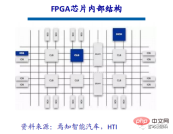
FPGA working principle
Because of FPGA It needs to be programmed repeatedly, and its basic structure to realize combinational logic cannot be completed through fixed NAND gates like ASIC, but can only adopt a structure that is easy to be configured repeatedly. Lookup tables can well meet this requirement. Currently, mainstream FPGAs all use lookup table structures based on SRAM technology. There are also some military and aerospace-grade FPGAs that use lookup table structures based on Flash or fuse and antifuse technology. Repeated configuration of FPGA is achieved by burning files to change the contents of the lookup table.
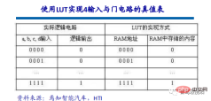
Look-Up-Table is referred to as LUT. LUT is essentially a RAM. Currently, 4-input LUTs are mostly used in FPGAs, so each LUT can be regarded as a RAM with 4-bit address lines. When the user describes a logic circuit through schematic diagram or HDL language, the PLD/FPGA development software will automatically calculate all possible results of the logic circuit and write the truth table (ie, the result) into RAM in advance. In this way, every time a signal is input Performing logical operations is equivalent to inputting an address, looking up the table, finding out the content corresponding to the address, and then outputting it.
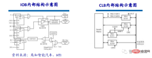
The programmable input/output unit, referred to as the I/O unit, is the interface part between the chip and the external circuit. It completes different Driving and matching requirements for input/output signals under electrical characteristics. The I/O within the FPGA is classified into groups, and each group can independently support different I/O standards. Through flexible configuration of the software, it can adapt to different electrical standards and I/O physical characteristics, adjust the drive current, and change the pull-up and pull-down resistors. At present, the frequency of I/O ports is getting higher and higher, and some high-end FPGAs can support data rates up to 2Gbps through DDR register technology.
CLB is the basic logic unit within FPGA. The actual number and characteristics of CLBs will vary from device to device, but each CLB contains a configurable switch matrix consisting of 4 or 6 inputs, some selection circuitry (multiplexers, etc.) and flip-flops composition. The switch matrix is highly flexible and can be configured to handle combinational logic, shift registers, or RAM. In Xilinx's FPGA devices, CLB consists of multiple (usually 4 or 2) identical Slices and additional logic. Each CLB module can not only be used to implement combinational logic and sequential logic, but can also be configured as distributed RAM and distributed ROM.
##The "core" killer of autonomous driving
The autonomous driving and advanced driver assistance systems (ADAS) market segments are undergoing a transformation, creating new and complex requirements for computing and sensor capabilities. FPGA has unique advantages that other chip solutions cannot match and is an excellent choice to meet the continuous development and changes of the autonomous driving industry. FPGA is a special technology in the chip field. On the one hand, it can be configured repeatedly through software tools, and on the other hand, it has rich IO interfaces and computing units. Therefore, FPGA can process pipeline parallelism and data parallelism at the same time according to the specific needs of the application scenario, and has the inherent advantages of high computing performance, low latency, and low power consumption.
FPGA has many advantages such as high throughput, high energy efficiency and real-time processing, which is very suitable for the technical requirements of autonomous driving. Standards and requirements for Advanced Assisted Driving Systems (ADAS) and In-Vehicle Experience (IVE) applications are evolving rapidly. The main concerns of system designers include excellent flexibility and faster development cycles while maintaining a higher performance-to-power ratio. . The combination of reprogrammable FPGAs and a growing portfolio of automotive-grade products enables automotive designers to meet design requirements and stay ahead of the ever-changing automotive industry.

A more adaptable platform
The real value for autonomous driving chips lies in the utilization of the computing engine, that is, the difference between theoretical performance and actual performance. FPGAs contain a large number of routing links as well as a large amount of small storage. The combination of these resources enables designers to create customized data feed networks for their compute engines for higher utilization levels. Programmable logic provides customers with a high degree of flexibility to adapt to the changing needs of emerging application areas such as ADAS and autonomous driving. Taking advantage of improved interface standards, algorithm innovation, and new sensor technologies all require adaptable platforms that can support not only software changes, but also hardware changes, and this is where FPGA chips excel.
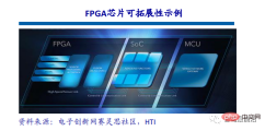
FPGA chips are scalable. Scalable chips change the amount of programmable logic, mostly in pin-compatible packages. This means developers can create a single ECU platform to host low, medium and high versions of ADAS feature packages and scale costs as needed by selecting the minimum density chip required.
##Differentiated Solutions
FPGA Chips allow developers to create unique, differentiated processing solutions that can be optimized for specific applications or sensors. This is not possible with ASSP chips, and even those that offer dedicated accelerators are limited in how they can be used and are available to essentially all competitors. Longtime Xilinx customers, for example, have created libraries of high-value IP that only they have access to, and those capabilities can be used across the company's various products. Starting from the 90nm node, Xilinx chips have been extremely cost-effective for high-volume automotive applications, with more than 160 million Xilinx chips used in the industry.

ASIC definition and characteristics
ASIC chips can be divided into TPU chips, DPU chips and NPU chips according to different terminal functions. Among them, TPU is a tensor processor dedicated to machine learning. For example, Google developed a programmable AI accelerator for the Tensorflow platform in May 2016. Its internal instruction set can run when the Tensorflow program changes or the algorithm is updated. DPU is Data Processing Unit, which can provide engines for computing scenarios such as data centers. NPU is a neural network processor that simulates human neurons and synapses at the circuit level and uses deep learning instruction sets to directly process large-scale electronic neuron and synapse data.ASIC has two design methods: full customization and semi-customization. Full customization relies on huge manpower and time costs to complete the entire integrated circuit design process in a completely independent manner. Although it is more flexible and better than semi-customized ASIC, its development efficiency is very low compared with semi-customized.

Performance improvement is obvious ASIC chips are very suitable for artificial intelligence application scenarios. For example, NVIDIA's first chip, Tesla P100, designed from scratch for deep learning, has a data processing speed 12 times that of its GPU series launched in 2014. Google's customized chip TPU for machine learning improves hardware performance to a level equivalent to that of current chips seven years after the development of Moore's Law. Just as CPUs changed the huge computers of the past, artificial intelligence ASIC chips will also significantly change the face of today's AI hardware devices. For example, the famous AlphaGo uses about 170 graphics processing units (GPUs) and 1,200 central processing units (CPUs). These devices require a computer room, high-power air conditioning, and multiple experts for system maintenance. And if all dedicated chips are used, it will most likely only require a space the size of an ordinary storage box, and the power consumption will be greatly reduced. The ASIC technology route is limited and open, and chip companies need to develop for mainstream networks, models, and operators related to driving. Under the same performance, the chip area is smaller, the cost is lower, and the power consumption is lower. The ASIC technology route will have great potential in the future. Choosing the ASIC route does not mean developing different ASICs for different models or performing different verifications. Because the functions that different car models need to implement are roughly the same, and the chip has limited access to models and operators, rapid iteration of the algorithm will not affect the chip's support for upper-layer functions. Car manufacturers cooperate with chip design companies to carry out differentiated customization, or a better choice. Because even with differentiated customization, 50% of the internal parts of the chip are universal. Chip design companies can carry out differentiated designs based on the original version to achieve some differentiated functions. FPGA is a product further developed on the basis of programmable devices such as PAL and GAL . It appears as a semi-custom circuit in the field of application-specific integrated circuits, which not only solves the shortcomings of custom circuits, but also overcomes the shortcomings of the limited number of gate circuits of the original programmable devices. Advantages: unlimited programming, relatively low latency, pipeline parallelism and data parallelism, the strongest real-time performance, and the highest flexibility. Disadvantages: It is difficult to develop, only suitable for fixed-point operations, and relatively expensive. Graphics processing unit (GPU), also known as display core, visual processor, display chip, is a type of processor specially used in personal computers, workstations, game consoles and some mobile devices (such as tablets). , mobile phones, etc.) that perform image and graphics-related operations. Advantages: It provides the basic structure of multi-core parallel computing, and has a large number of cores, which can support parallel computing of large amounts of data and has higher floating-point computing capabilities. Disadvantages: management control capability (weakest), power consumption (highest). ASIC, or application specific integrated circuit, refers to an integrated circuit designed and manufactured in response to specific user requirements and the needs of specific electronic systems. Currently, one of the most popular ways to design ASIC is with CPLD (Complex Programmable Logic Device) and FPGA (Field Programmable Logic Array). Advantages: As a product of integrated circuit technology and the complete machine or system technology of a specific user, it has smaller size, lighter weight, lower power consumption, improved reliability, improved performance and confidentiality compared with general-purpose integrated circuits. Enhancement, cost reduction and other advantages. Disadvantages: Insufficient flexibility and more expensive than FPGA. Comparison of mainstream architecture solutions: three mainstream architectures

Limitations of computing power theory: TOPS computing power is not completely equal to actual performance
With the rise of ADAS, autonomous driving technology, and the gradual deepening of software-defined cars, the demand for computing power and massive data processing capabilities of smart cars has skyrocketed, and the chip "stack" of traditional cars has "The solution can no longer meet the computing power needs of autonomous driving. The chip ultimately serves the in-vehicle computing platform of the car company. In the case of "software-defined cars", solving the support problem of the intelligent driving system computing platform cannot be achieved only by stacking chip computing power.
The chip is the stage for software. The standard for measuring the quality of a chip depends on whether the software on the chip can maximize its function. There needs to be an effective match between computing power and software. When comparing two chips with the same computing power, the chip that allows the software to run more efficiently is the “good chip”. The most important factors that determine the true value of computing power are memory (SRAM and DRAM) bandwidth, as well as the actual operating frequency (i.e., supply voltage or temperature), and the batch size of the algorithm.
A single chip’s computing power TOPS is a key indicator, but it is not the only one. Autonomous driving is a complex system that requires vehicle-road, cloud-edge collaboration. Therefore, in addition to the core, its competition also includes software and hardware synergy, platforms, tool chains, etc. The infinite expansion of chip computing power and embedded hardware will not be the future trend, and the hardware also needs to match the actual situation. Behind the high is the problem of high power consumption and low utilization.

Event Camera Introduction
Introduction and working mechanism
Event cameras are inspired by the vision of the human eye and animals, also known as silicon retina. Biological vision is only sensitive to areas with changes, and event cameras capture the occurrence of events or changes. ,
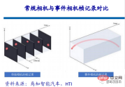
In the traditional visual field, the information returned by the camera is synchronized. The so-called synchronization means that at a certain time t, the camera will expose all the pixels at this time. Fill in a matrix and send it back to generate a photo. All pixels in a photo correspond to the same moment. As for video, it is just a picture of many frames. The time interval between adjacent pictures can be large or small. This is the frame rate (frame rate), also called time delay (time latency). Event cameras are similar to the human brain and eyes, skipping irrelevant background and directly sensing the core of a scene, creating pure events rather than data.
The working mechanism of the event camera is that when the brightness of a certain pixel changes to a certain threshold, the camera will return an event in the above format, of which the first two items is the pixel coordinate of the event, the third item is the timestamp of the event, and the last item is the polarity (polarity) 0, 1 (or -1, 1), which represents whether the brightness is from low to high or from high to low. .
In this way, within the entire camera field of view, as long as there is a change in pixel value, an event will be returned. All these events occur asynchronously (no matter how small the time interval is) It is impossible to be completely simultaneous), so the timestamps of the events are different. Because the return is simple, compared with traditional cameras, it has the characteristics of low latency and can capture pixel changes within a short time interval. The delay is micro. Seconds.
##Application in the field of autonomous driving
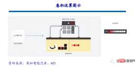
The visual recognition algorithms used in the field of autonomous driving today are basically based on convolutional neural networks. The operation of the visual algorithm is essentially a convolution operation. This kind of calculation is not complicated. In essence, it only involves addition, subtraction, multiplication and division, which is a kind of multiplication, accumulation and accumulation operations. However, such simple operations exist in large quantities in convolutional neural networks, which places high demands on the performance of the processor.
Take ResNet-152 as an example. This is a 152-layer convolutional neural network. The amount of calculations required to process a 224*224 image is approximately 22.6 billion times. , if this network wants to process a 1080P 30-frame camera, the computing power it requires is as high as 33 trillion times per second, which is very huge.
##Save computing power by reducing invalid calculations
99% of visual data in the field of autonomous driving is useless background in AI processing. For example, when detecting ghost probes, the changed area is only a small part, but traditional visual processing still has to process 99% of the background areas that do not change, which not only wastes a lot of computing power, but also wastes time. Or if there is a diamond in the gravel, the AI chip and traditional cameras need to identify each grain of sand and screen out the diamonds, but humans can detect the diamonds by just looking at them. The AI chip and traditional cameras take more time than humans. 100 times or 1000 times.In addition to the advantages of reduced redundant information and almost no delay, the advantages of event cameras are also due to low latency. When shooting high-speed objects, traditional cameras will blur due to a period of exposure time, while event cameras Cameras barely do. In addition, the event camera has a truly high dynamic range. Due to the characteristics of the event camera, traditional cameras will be "blind" in environments with strong or weak light intensity, but the pixel changes will still exist, so the event camera can still see clearly. s things.
The above is the detailed content of An overview of the three mainstream chip architectures for autonomous driving in one article. For more information, please follow other related articles on the PHP Chinese website!
 How to Run LLM Locally Using LM Studio? - Analytics VidhyaApr 19, 2025 am 11:38 AM
Running large language models at home with ease: LM Studio User Guide In recent years, advances in software and hardware have made it possible to run large language models (LLMs) on personal computers. LM Studio is an excellent tool to make this process easy and convenient. This article will dive into how to run LLM locally using LM Studio, covering key steps, potential challenges, and the benefits of having LLM locally. Whether you are a tech enthusiast or are curious about the latest AI technologies, this guide will provide valuable insights and practical tips. Let's get started! Overview Understand the basic requirements for running LLM locally. Set up LM Studi on your computer
 Guy Peri Helps Flavor McCormick's Future Through Data TransformationApr 19, 2025 am 11:35 AM
Guy Peri is McCormick’s Chief Information and Digital Officer. Though only seven months into his role, Peri is rapidly advancing a comprehensive transformation of the company’s digital capabilities. His career-long focus on data and analytics informs
 What is the Chain of Emotion in Prompt Engineering? - Analytics VidhyaApr 19, 2025 am 11:33 AM
Introduction Artificial intelligence (AI) is evolving to understand not just words, but also emotions, responding with a human touch. This sophisticated interaction is crucial in the rapidly advancing field of AI and natural language processing. Th
 12 Best AI Tools for Data Science Workflow - Analytics VidhyaApr 19, 2025 am 11:31 AM
Introduction In today's data-centric world, leveraging advanced AI technologies is crucial for businesses seeking a competitive edge and enhanced efficiency. A range of powerful tools empowers data scientists, analysts, and developers to build, depl
 AV Byte: OpenAI's GPT-4o Mini and Other AI InnovationsApr 19, 2025 am 11:30 AM
This week's AI landscape exploded with groundbreaking releases from industry giants like OpenAI, Mistral AI, NVIDIA, DeepSeek, and Hugging Face. These new models promise increased power, affordability, and accessibility, fueled by advancements in tr
 Perplexity's Android App Is Infested With Security Flaws, Report FindsApr 19, 2025 am 11:24 AM
But the company’s Android app, which offers not only search capabilities but also acts as an AI assistant, is riddled with a host of security issues that could expose its users to data theft, account takeovers and impersonation attacks from malicious
 Everyone's Getting Better At Using AI: Thoughts On Vibe CodingApr 19, 2025 am 11:17 AM
You can look at what’s happening in conferences and at trade shows. You can ask engineers what they’re doing, or consult with a CEO. Everywhere you look, things are changing at breakneck speed. Engineers, and Non-Engineers What’s the difference be
 Rocket Launch Simulation and Analysis using RocketPy - Analytics VidhyaApr 19, 2025 am 11:12 AM
Simulate Rocket Launches with RocketPy: A Comprehensive Guide This article guides you through simulating high-power rocket launches using RocketPy, a powerful Python library. We'll cover everything from defining rocket components to analyzing simula


Hot AI Tools

Undresser.AI Undress
AI-powered app for creating realistic nude photos

AI Clothes Remover
Online AI tool for removing clothes from photos.

Undress AI Tool
Undress images for free

Clothoff.io
AI clothes remover

Video Face Swap
Swap faces in any video effortlessly with our completely free AI face swap tool!

Hot Article

Hot Tools

SublimeText3 English version
Recommended: Win version, supports code prompts!

VSCode Windows 64-bit Download
A free and powerful IDE editor launched by Microsoft

SAP NetWeaver Server Adapter for Eclipse
Integrate Eclipse with SAP NetWeaver application server.

SublimeText3 Linux new version
SublimeText3 Linux latest version

Dreamweaver CS6
Visual web development tools


