
 Technology peripheralsIt IndustrySamsung's 9th generation V-NAND metal wiring mass production process is revealed to use molybdenum technology for the first time
Samsung's 9th generation V-NAND metal wiring mass production process is revealed to use molybdenum technology for the first time

This website reported on July 3 that according to Korean media The Elec, Samsung tried to use molybdenum (Mo) for the first time in the "metal wiring" of its 9th generation V-NAND.

- Wafer manufacturing
- Oxidation
- Photolithography
- Etching
- Deposition
- Metal wiring
- Testing
- Packaging
Metal The wiring process mainly uses different methods to connect billions of electronic components to form different semiconductors (CPU, GPU, etc.), which can be said to "inject life into semiconductors."
Sources saySamsung has introduced five Mo deposition machines from Lam Research Company, and plans to introduce 20 more equipment next year.
In addition to Samsung Electronics, companies such as SK Hynix, Micron and Kioxia are also considering using molybdenum. Unlike tungsten hexafluoride (WF6) used in the existing NAND process, the molybdenum precursor (molybdenum precursor) is solid and must be sublimated directly into a gaseous state at a high temperature of 600°C. This process requires separate deposition equipment. .
Samsung reported in May this year that it had started mass production of the first batch of ninth-generation V-NAND flash memory, with the bit density increased by about 50% compared to the eighth-generation V-NAND.
The ninth-generation V-NAND is equipped with the next-generation NAND flash interface "Toggle 5.1", which can increase data input/output speed by 33%, up to 3.2 gigabits per second (Gbps). In addition to this new interface, Samsung also plans to solidify its position in the high-performance SSD market by expanding support for PCIe 5.0.
The above is the detailed content of Samsung's 9th generation V-NAND metal wiring mass production process is revealed to use molybdenum technology for the first time. For more information, please follow other related articles on the PHP Chinese website!

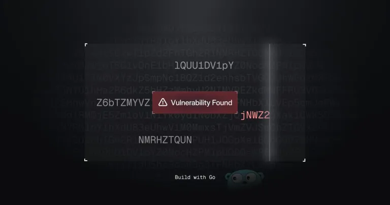 Building a Network Vulnerability Scanner with GoApr 01, 2025 am 08:27 AM
This Go-based network vulnerability scanner efficiently identifies potential security weaknesses. It leverages Go's concurrency features for speed and includes service detection and vulnerability matching. Let's explore its capabilities and ethical
 Top 10 Best Free Backlink Checker Tools in 2025Mar 21, 2025 am 08:28 AM
Website construction is just the first step: the importance of SEO and backlinks Building a website is just the first step to converting it into a valuable marketing asset. You need to do SEO optimization to improve the visibility of your website in search engines and attract potential customers. Backlinks are the key to improving your website rankings, and it shows Google and other search engines the authority and credibility of your website. Not all backlinks are beneficial: Identify and avoid harmful links Not all backlinks are beneficial. Harmful links can harm your ranking. Excellent free backlink checking tool monitors the source of links to your website and reminds you of harmful links. In addition, you can also analyze your competitors’ link strategies and learn from them. Free backlink checking tool: Your SEO intelligence officer


Hot AI Tools

Undresser.AI Undress
AI-powered app for creating realistic nude photos

AI Clothes Remover
Online AI tool for removing clothes from photos.

Undress AI Tool
Undress images for free

Clothoff.io
AI clothes remover

AI Hentai Generator
Generate AI Hentai for free.

Hot Article
Hot Tools

Dreamweaver CS6
Visual web development tools

Safe Exam Browser
Safe Exam Browser is a secure browser environment for taking online exams securely. This software turns any computer into a secure workstation. It controls access to any utility and prevents students from using unauthorized resources.

EditPlus Chinese cracked version
Small size, syntax highlighting, does not support code prompt function

Zend Studio 13.0.1
Powerful PHP integrated development environment

WebStorm Mac version
Useful JavaScript development tools

