


According to news from this website on August 15, the second phase expansion plan of TSMC’s Zhongke Taichung Park was originally planned to start this year. However, the Zhongke Administration Bureau has postponed the approval time of the expansion development plan three times. The specific time when it will be approved is still unclear. Confirmed
The China Science and Technology Administration Bureau received a notification from the Taichung City Government today that the second phase expansion project of the China Science and Technology Taichung Park regarding TSMC’s 2nm plant has been scheduled on the urban plan review agenda on the 25th of this month

Director Xu Maoxin said that due to the delay of one and a half years in the expansion case, the original operation plan could no longer be completed on time. In addition, the government still needs to go through the review of the Metropolitan Committee of the Interior Ministry, and it is expected that the land use will not be started until the end of the year. Therefore, the land handover cannot be determined by the end of this year.
According to reports, due to the delay of the second phase expansion project of the Taichung Park of China Science and Technology TSMC had to decide to build a 2nm production line in Kaohsiung factory
In view of the recent rapid growth and strong performance of AI business opportunities, manufacturers including chip giants such as Apple and Nvidia have shown strong interest in TSMC’s 2nm process Interest, so TSMC decided to put the Kaohsiung factory directly into the 2nm process. In addition, Mr. Huang Renxun has also stated that the future generation of server chips will fully adopt TSMC’s 2nm process
According to our understanding, TSMC plans to build a major 2nm production plant in Baoshan, Hsinchu, which is internally named Fab 20 plans to build four factory buildings from P1 to P4. Currently, the P1 factory is advancing intensively and is expected to conduct risky trial production next year and start mass production in the second half of 2025. According to TSMC supply chain sources, TSMC has notified equipment manufacturers that it plans to start mass production in the second half of 2025. Delivery of 2nm related machines will begin in the third quarter of next year. It is expected that the 2nm installation operation of the Kaohsiung plant will be one month later than that of the Hsinchu Baoshan plant.
TSMC plans to build two 12-inch wafer fabs at the former site of CNPC Kaohsiung Refinery. The first phase will include a monthly production capacity of 40,000 wafers. 7nm and 6nm wafer fabs, the second phase will include 28nm and 22nm wafer fabs with a monthly production capacity of 20,000 pieces. The first phase of the fab is expected to be completed in 2024 and mass production will begin in 2025. However, due to various reasons, it seems that we are currently considering entering the 2nm project, and the specific plan has not yet been determined
All articles on this site contain advertising statements, including external jump links (such as hyperlinks, QR codes, passwords and other forms), aiming to convey more information and save selection time, the results are for reference only
The above is the detailed content of TSMC's Zhongke 2nm plant will be postponed until next year.. For more information, please follow other related articles on the PHP Chinese website!

 计划 2025 年商用,报道称台积电组建 200 人研究团队推进硅光子技术Oct 05, 2023 pm 03:13 PM
本站10月5日消息,根据集邦咨询报道称,台积电目前正和英伟达、博通等主要客户合作,组建了超过200名研究人员的硅光子技术团队,目标在2024年下半年完成该项目,并于2025年开始投入商用。报道称台积电的紧凑型通用光子引擎(COUPE),提供光子IC(PIC)与电子IC(EIC)异质整合,降低40%的能耗,有望大幅提升客户的采用意愿。PIDA执行长罗怀家表示,硅光子技术一直以来都是光电领域的重要关注点,光电产品正朝着轻薄、小巧、节能、省电的方向发展硅光子及共同封装光学元件(CPO)成为业界新显学,
 联发科和台积电是什么关系?Nov 13, 2022 pm 03:56 PM
联发科和台积电都是中国台湾公司,台积电是联发科晶圆供应商之一;联发科是全球著名IC设计厂商,专注于无线通讯及数字多媒体等技术领域;台积电属于半导体制造公司,成立于1987年,是全球第一家专业积体电路制造服务企业,总部与主要工厂位于台湾新竹科学园区。
 台积电全称叫什么Oct 27, 2022 pm 04:37 PM
台积电全称叫“台湾积体电路制造股份有限公司”,属于半导体制造公司,成立于1987年,是全球第一家专业积体电路制造服务(晶圆代工foundry)企业;该公司经营的是集成电路制造,为客户生产的晶片涵盖电脑产品、通讯产品、消费性、工业用及标准类半导体等众多电子产品应用领域。
 消息称台积电先进封装客户大幅追单,明年月产能拟拉升 120%Nov 13, 2023 pm 12:29 PM
本站11月13日消息,据台湾经济日报,台积电CoWoS先进封装需求迎来爆发,除英伟达已经在10月确定扩大订单外,苹果、AMD、博通、Marvell等重量级客户近期同样大幅追单。据报道,台积电正在努力加快扩大CoWoS先进封装产能,以满足上述五大客户的需求。预计明年的月产能将比原先的目标增加约20%,达到3.5万片分析人士表示,台积电的五个主要客户纷纷下大单,这表明人工智能应用已经广泛普及,各大厂商对于人工智能芯片的需求大幅增加本站查询发现,当前CoWoS先进封装技术主要分为三种——CoWos-S
 181.2 亿美元,英伟达超过台积电和英特尔,坐上芯片行业收入第一宝座Nov 25, 2023 pm 12:27 PM
本站11月25日消息,金融分析师丹・奈斯泰特(DanNystedt)近日指出,基于2023年第3季度各家财报数据,英伟达超过台积电和英特尔,坐上芯片行业收入第一宝座。英伟达第三财季营收为181.20亿美元(本站备注:当前约1293.77亿元人民币),与上年同期的59.31亿美元相比增长206%,与上一财季的135.07亿美元相比增长34%。英伟达第三财季净利润为92.43亿美元(当前约659.95亿元人民币),与上年同期的6.80亿美元相比增长1259%,与上一财季的61.88亿美元相比增长49
 台积电第三季度净利润 2108 亿元新台币,同比下降 25%Oct 19, 2023 pm 03:13 PM
本站10月19日消息,台积电10月19日公布第三季度业绩,第三季度净营收5467.3亿元新台币,同比下降10.8%,环比增长13.7%;第三季度净利润2108.0亿元新台币,同比下降25.0%,环比增长16.0%。台积电本季度毛利率为54.3%,营业利润率为41.7%,净利润率为38.6%。第三季度,3纳米的出货量占总晶圆收入的6%;5纳米占37%;7纳米占16%。台积电表示,第三季度资本支出为71亿美元,上一季度为81.7亿美元。台积电在台北上市的股价在2022年下跌了27.1%,但今年迄今已
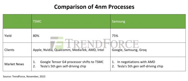 AMD正在与三星洽谈迁移部分订单,谷歌Tensor G4将改为使用台积电Nov 14, 2023 pm 01:45 PM
本站11月14日消息,gamma0burst深挖曝光的信息显示,AMD即将推出的“Prometheus”CPU,采用Zen5c核心,会同时交由三星4nm和台积电3nm工艺量产。据报道,考虑到AMD等用户的需求,他们的关注已经从工艺节点、生产良率和成本等因素扩展到了产能和生态链等多个方面报道称三星正积极扩展4nm工艺,希望从台积电手中吸引更多的订单。目前关于良率的信息,业内人士认为台积电4nm工艺良率为80%,而三星从今年年初的50%增加到了75%,媲美台积电。外界猜测高通、英伟达等大客户可能会回
 台积电董事会核准以不超 1 亿美元认购 Arm 股份Sep 16, 2023 pm 08:25 PM
根据台积电官网消息,本站获悉,台积电于9月12日召开了一次临时董事会,并做出了以下重要决议:一、核准将IntelCorporation获得IMSNanofabricationGlobal,LLC10%股权的额度限制在不超过4.328亿美元(约合31.59亿元人民币)之内核准认购ArmHoldingsplc普通股股份的额度不超过1亿美元(约合7.3亿元人民币),认购价格将根据该公司首次公开发行的最终价格确定根据消息,Arm将在本周上市,目前正在进行前期认购。然而,由于需求火爆,可能导致投行提前一天


Hot AI Tools

Undresser.AI Undress
AI-powered app for creating realistic nude photos

AI Clothes Remover
Online AI tool for removing clothes from photos.

Undress AI Tool
Undress images for free

Clothoff.io
AI clothes remover

AI Hentai Generator
Generate AI Hentai for free.

Hot Article
Hot Tools

Zend Studio 13.0.1
Powerful PHP integrated development environment

SublimeText3 English version
Recommended: Win version, supports code prompts!

Dreamweaver Mac version
Visual web development tools

ZendStudio 13.5.1 Mac
Powerful PHP integrated development environment

Dreamweaver CS6
Visual web development tools

