
 Hardware TutorialHardware NewsAMD 'Strix Halo” Zen 5 APU package exposure: RDNA 3.5 graphics die area 307 square millimeters
News from this site on August 1st. The source @7931doomer111 tweeted today (August 1st) and shared information about AMD “Strix Halo” Zen 5 APU, showing that the graphics die size equipped with RDNA 3.5 is 307 square millimeters. .

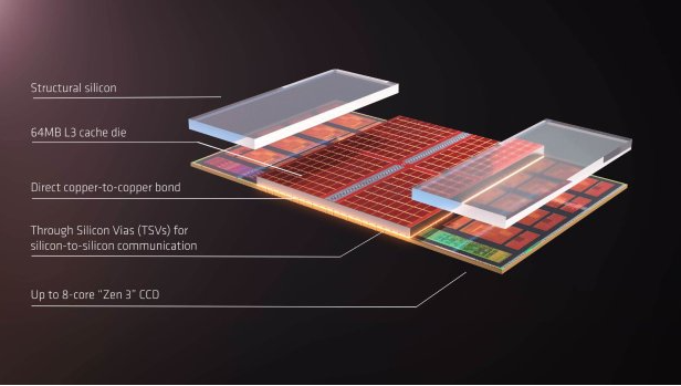
According to the exposed information, AMD “Strix Halo” Zen 5 APU adopts FP11 package with a package area of 37.5*45 mm, which is the same as the LGA-1700 slot panel.

The infographic shows that the largest Die is a graphics module, using RDNA 3.5 graphics technology, with an area of at least 307 square millimeters, while the smaller Die has 2 CCDs (each providing 8 Zen 5 core), measuring 66.3 square millimeters.
Another exposed picture is attached to this site, which reveals the thermal design data of AMD “Strix Halo” Zen 5 APU, including 55W, 85W and 120W (excluding memory power consumption). AMD estimates memory power consumption at 9W for a 32GB system and 13W for a 128GB system.

The above is the detailed content of AMD 'Strix Halo” Zen 5 APU package exposure: RDNA 3.5 graphics die area 307 square millimeters. For more information, please follow other related articles on the PHP Chinese website!

 修复:Windows 11 中未安装 AMD 显卡驱动程序错误May 03, 2023 am 09:13 AM
在配备AMDGPU的Windows11PC上出现未安装AMD显卡驱动程序错误。这是某些用户在选择AMDRadeon设置上下文菜单选项时发生的错误。弹出此错误消息,而不是打开AMDRadeon设置:未安装AMD显卡驱动程序,或AMD驱动程序无法正常运行。请安装适合您的AMD硬件的AMD驱动程序。该错误消息突出显示了AMD图形驱动程序的问题。这通常意味着PC具有过时、不兼容或损坏的AMD驱动程序。这是您可以修复Windows11中未安装AMD
 amd radeon software是什么Feb 21, 2023 am 11:58 AM
amd radeon software是显卡的驱动程序,是用于Advanced Micro Devices的显卡和APU的设备驱动程序和实用程序软件包。Radeon Software驱动不只是包含显卡驱动程序,实际上还包含设置及问题报告向导、HDMI音频驱动等,如果不想对显卡做各种设置。除了识别显卡信息,Radeon Software还能识别显示器并提供丰富的显示器设置功能。
 AMD RX 7800M XT在3DMark测试中获得高分,可与桌面端RTX 4070媲美Jun 07, 2023 pm 11:45 PM
6月7日消息,根据最新报道,AMD公司的移动显卡AMDRadeonRX7800MXT首次公布了其在3DMark跑分测试中的成绩,显示该显卡性能将超越上一代的RX6800。据可靠消息源透露,还有其他基于Navi32核心的AMD移动显卡规格被曝光,这也是用于AMDRadeonRX7700/7800系列的Navi32芯片首次亮相。从跑分结果来看,在TimeSpy测试中,AMDRX7800MXT获得了17842的分数,与桌面端的RTX4070显卡的表现相当(IT之家注:RTX4070分数为17736,而
 怎样从 Windows 11 下载 AMD 显卡驱动程序May 09, 2023 pm 09:52 PM
使用图形处理单元(GPU)或显卡在Windows11计算机上显示图形。因此,今天我们将了解如何在Windows11上下载AMD显卡驱动程序。内置的任务管理器软件是确定您的计算机正在使用哪个显卡以及当前使用了多少电量的最简单、最准确的方法。跟随我们将首先看看如果您从PC中删除AMD软件会发生什么,然后跳转到您可以在Windows11设备上下载图形驱动程序的方法列表。如果我删除AMD软件会怎样?AMDRadeon设置是主要的驱动程序界面,允许用户更改图形驱动程序的许多
 由于 fTPM 错误,AMD PC 在 Windows 10 和 11 上出现卡顿,临时解决方法May 13, 2023 pm 07:04 PM
一两个月以来,AMD的Ryzen处理器被发现在启用固件TPM(fTPM)的Windows10和11系统上卡顿(通过Reddit)或冻结。今天,AMD在确定导致这些问题的原因后发布了一份公告。据该公司称,挂起和卡顿是由串行外设接口(SPI)闪存ROM内的扩展内存事务操作引起的。AMD已确定,选定的AMDRyzen™系统配置可能会间歇性地在位于主板上的SPI闪存(“SPIROM”)中执行与fTPM相关的扩展内存事务,这可能导致系统交互性或响应性暂时暂
 AMD发布Ryzen 7000系列新成员:Ryzen 5 7500F处理器Jul 20, 2023 pm 12:01 PM
7月11日消息,据知情人士透露,AMD公司计划在中国市场推出一款全新处理器型号,名为AMDRyzen57500F。该处理器被认为是Ryzen7000系列中的一员,相较于Ryzen57600,7500F不包含集成的核显。这一消息显示,AMD将首先在中国发布Ryzen57500F处理器,并且暂无计划将其引入美国市场。AMDRyzen57500F处理器采用了Ryzen7000系列的制造工艺,而非像Ryzen57600一样采用了APU芯片。据了解,该处理器将于本月底面向中国市场的零售商和电商平台发布,并
 突破性的AMD原型处理器亮相:锐龙9 5900X3D震撼亮相Jun 20, 2023 pm 03:55 PM
6月20日消息,近期,AMD在其奥斯汀总部向少数媒体展示了一款令人惊叹的原型产品,名为“锐龙95900X3D”。这款处理器采用了最新的3DV-Cache缓存技术,为AMD的锐龙产品线带来了显著的性能提升。据了解,这款“锐龙95900X3D”处理器集成了12个Zen4核心和128MB的3D缓存。在Windows任务管理器中,该处理器显示出192MB的三级缓存(128MB3D缓存+64MB原生缓存),以及6MB的二级缓存和768KB的一级缓存,总共达到了198.75M
 2022 年 12 月星期二补丁日触发 AMD 锐龙 PC 上的冻结问题Apr 13, 2023 pm 07:28 PM
以防万一您还不知道,11 月的周二补丁日更新修复了与大多数 AMD 处理器上的 Spectre 变体 2 相关的安全漏洞。话虽如此,12 月的下一次跟进,即 2022 年的最后一次跟进,显然在配备 AMD CPU 的系统上并不是最好的。为什么?好吧,因为一些用户报告了其AMD Ryzen系统上的冻结问题。这似乎发生在带有KB11更新的Windows 11 22H2上5021255。Windows 11 版本 22H2 上出现问题老实说,这不是微软第一次或最后一次使用旨在实际改进它的补丁来破坏系统


Hot AI Tools

Undresser.AI Undress
AI-powered app for creating realistic nude photos

AI Clothes Remover
Online AI tool for removing clothes from photos.

Undress AI Tool
Undress images for free

Clothoff.io
AI clothes remover

AI Hentai Generator
Generate AI Hentai for free.

Hot Article
Hot Tools

WebStorm Mac version
Useful JavaScript development tools

SublimeText3 Mac version
God-level code editing software (SublimeText3)

SublimeText3 Chinese version
Chinese version, very easy to use

Safe Exam Browser
Safe Exam Browser is a secure browser environment for taking online exams securely. This software turns any computer into a secure workstation. It controls access to any utility and prevents students from using unauthorized resources.

Dreamweaver Mac version
Visual web development tools

